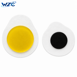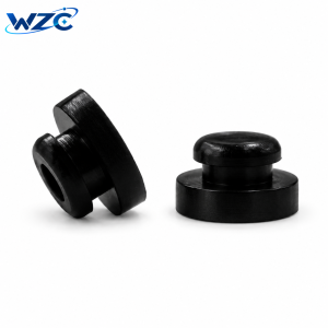
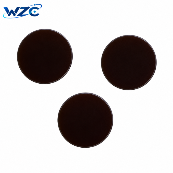
High-Temperature Bionic Wafer Handling Pad
The High-Temperature Bionic Wafer Handling Pad is designed
for semiconductor wafer and substrate handling in elevated-temperature
process environments.
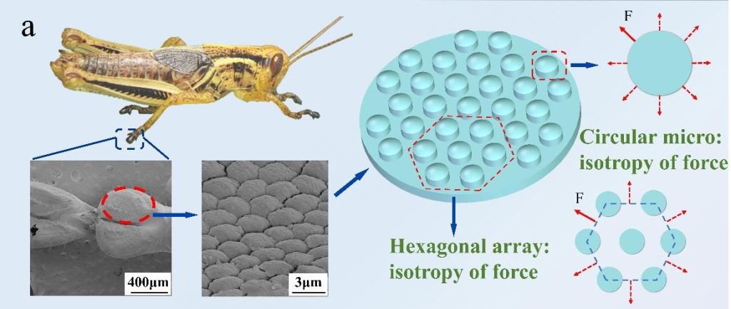
Its biomimetic microstructured contact surface provides
high tangential friction with relatively low normal adhesion,
helping reduce wafer slip while maintaining controlled release during transfer,
positioning and handling.
Different material systems are available according to the operating temperature.
Standard high-temperature pad materials can be used for direct-contact
temperatures around 250–270°C, while
FFKM-based pad solutions up to 400°C can be evaluated
for higher-temperature applications.
High Friction and Low Adhesion at Elevated Temperature
The microstructured contact surface is designed to maintain stable lateral friction
between the wafer and the handling pad without relying on excessive normal adhesion.
This helps provide stable substrate support during acceleration, deceleration,
alignment and transfer while reducing sticking during wafer release.
Temperature Options
Material selection should be based on the actual process temperature,
contact time, atmosphere and chemical environment.
| Material Option | Typical Temperature Capability | Typical Use |
|---|---|---|
| Standard High-Temperature Material | Up to approx. 250°C direct contact | General elevated-temperature wafer handling |
| Enhanced High-Temperature Material | Up to approx. 270°C direct contact | Higher-temperature semiconductor handling |
| FFKM Pad | Up to 400°C | High-temperature process environments |
FFKM High-Temperature Pad
For demanding thermal environments, an
FFKM high-temperature friction pad can be supplied.
FFKM material provides improved thermal and chemical resistance compared
with standard elastomer-based pad materials.
The high-temperature version is suitable for applications where conventional
wafer handling pads cannot meet the required thermal exposure conditions.
Because actual performance depends on temperature, contact duration,
process atmosphere and chemical exposure, the operating condition should be
confirmed before final material selection.
Key Features
- High tangential friction for stable wafer handling
- Low normal adhesion for controlled substrate release
- Suitable for elevated-temperature semiconductor environments
- Standard high-temperature and FFKM material options
- Direct-contact temperature options around 250°C, 270°C and up to 400°C
- Low surface marking and residue
- Microstructured contact surface
- Custom pad dimensions and geometry
- Custom mounting structures available
Typical Applications
High-temperature bionic friction pads can be used in semiconductor and
substrate handling equipment operating under elevated-temperature conditions.
- High-temperature wafer handling robots
- Semiconductor process equipment
- Wafer transfer systems
- Robot fingers and end effectors
- Heated substrate handling
- High-temperature alignment systems
- Vacuum and atmospheric handling environments
- Custom semiconductor automation equipment
Custom High-Temperature Pad Solutions
High-temperature wafer handling pads can be customized according to
equipment structure and process conditions.
- Custom pad diameter
- Custom thickness
- Custom round, ring or special geometry
- Custom mounting structure
- Embedded or other mechanical mounting designs
- FFKM material option
- Custom contact height
- Wafer or substrate size requirements
- Operating temperature requirements
- Vacuum or atmospheric environment requirements
For technical evaluation, please provide the operating temperature,
contact time, substrate size, mounting structure, atmosphere
and any relevant chemical exposure information.
Material Selection for High-Temperature Applications
The correct pad material should be selected according to the actual
working environment rather than temperature alone.
Important evaluation parameters include:
- Maximum operating temperature
- Continuous or intermittent thermal exposure
- Direct wafer contact temperature
- Vacuum or atmospheric environment
- Chemical and plasma exposure
- Required friction performance
- Required pad lifetime
Handling and Maintenance
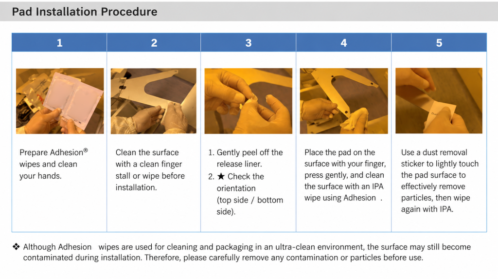
- Handle pads in a clean environment whenever possible.
- Wear clean gloves during installation and maintenance.
- Do not touch the microstructured contact surface with sharp tools.
- Avoid strong rubbing with abrasive materials.
- Keep the pad surface free from particles and contamination.
- Confirm the pad material is suitable for the required temperature before use.
- Inspect the pad periodically in high-temperature applications.
Frequently Asked Questions
What is a high-temperature wafer handling pad?
It is a friction pad designed to maintain stable wafer contact and handling
performance in elevated-temperature semiconductor process environments.
What temperature can the pad withstand?
Standard high-temperature materials are available for direct-contact
temperatures around 250°C and 270°C. FFKM-based pad solutions can be
evaluated for applications up to 400°C.
Is FFKM available?
Yes. FFKM high-temperature pad solutions are available for more demanding
thermal environments.
Can the pad size be customized?
Yes. Diameter, thickness, geometry and mounting structure can be customized
according to the wafer handling equipment.
Can it be used in vacuum environments?
High-temperature pad solutions can be evaluated for both vacuum and
atmospheric environments. Please provide the actual process conditions
when requesting a quotation.
What information is required for quotation?
Please provide the required pad dimensions, operating temperature,
contact time, substrate size, mounting structure, operating atmosphere
and any relevant chemical or plasma exposure conditions.