12 Inch 4H-N SiC Wafer Specifications
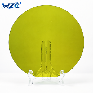
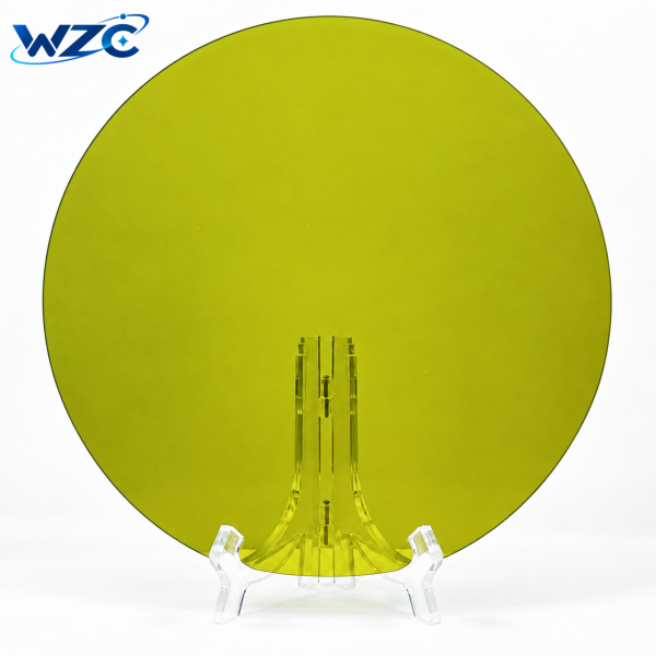
The 12 Inch 4H-N SiC Wafer is a 300 mm N-type 4H silicon carbide substrate
with a nominal diameter of 300.00 ± 0.5 mm and a standard thickness of
700 ± 50 μm.
The substrate is specified with a 4.0° crystal orientation toward
<11-20> ±0.5°. Both the Si face and C face are CMP polished.
| Parameter | Specification |
|---|---|
| Material | 4H Silicon Carbide (4H-SiC) |
| Conductivity Type | N-Type |
| Diameter | 300.00 ± 0.5 mm |
| Thickness | 700 ± 50 μm |
| Crystal Orientation | 4.0° toward <11-20> ±0.5° |
| Notch Depth | 1.0–1.25 mm |
| Notch Orientation | <1-100> ±5° |
| Si Face | CMP Polished |
| C Face | CMP Polished |
| Laser Marking | C Face, above the notch |
| Area Contamination | None on both faces |
| Edge Profile | Chamfer, R-Shape |
| Packaging | Multi-wafer cassette or single wafer container |
12 Inch 4H-N Silicon Carbide Wafer Overview
The 12 Inch 4H-N SiC Wafer, also referred to as a
300 mm N-type SiC substrate, is a large-diameter 4H silicon carbide
substrate with controlled diameter, thickness, crystal orientation and surface processing.
The standard substrate diameter is 300.00 ±0.5 mm,
with a thickness of 700 ±50 μm. The wafer is specified
with a 4.0° orientation toward <11-20> ±0.5°.
300 mm 4H-N SiC Substrate
The 12 inch substrate uses 4H-SiC with N-type conductivity.
The large 300 mm wafer format provides a platform for applications and process
development requiring large-diameter silicon carbide substrates.
Electrical and defect-related parameters should be confirmed according to the
specific order and applicable product specification.
4° Crystal Orientation
The 12 inch 4H-N SiC wafer is specified with a crystal orientation of
4.0° toward <11-20> ±0.5°.
A notch is used for wafer orientation, with a specified notch depth of
1.0–1.25 mm and notch orientation of
<1-100> ±5°.
Double-Side CMP Surface
Both the Si face and C face of the
12 inch SiC substrate are specified as CMP polished.
The current product specification also requires no area contamination on
either wafer face.
Laser Marking and Edge Profile
Laser marking is located on the C face above the notch.
The wafer edge is processed with a chamfered R-shape profile.
How SiC Wafers Are Manufactured
SiC wafer manufacturing generally involves crystal growth, crystal orientation,
wafer slicing, grinding, polishing, chemical mechanical polishing (CMP),
cleaning and final inspection.
These processing stages are used to control wafer dimensions, orientation,
surface condition and edge quality before final inspection and packaging.
Packaging
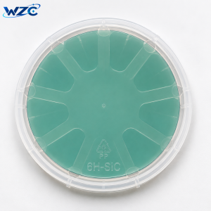
12 inch 4H-N SiC wafers can be supplied in a
multi-wafer cassette or single wafer container
according to order quantity and packaging requirements.
Custom 12 Inch 4H-N SiC Wafer Requirements
For quotation and technical evaluation, please provide the required quantity
and any specific requirements for electrical properties, wafer geometry,
surface quality, defect limits or inspection criteria.
Parameters not listed in the standard specification can be confirmed according
to the specific project requirements.
Frequently Asked Questions
What is a 12 Inch 4H-N SiC Wafer?
It is a large-diameter N-type 4H silicon carbide substrate with a nominal
diameter of 300 mm.
What is the diameter of the 12 inch SiC substrate?
The specified diameter is 300.00 ±0.5 mm.
What is the standard thickness?
The specified standard thickness is 700 ±50 μm.
What is the crystal orientation?
The specified crystal orientation is
4.0° toward <11-20> ±0.5°.
Are both sides CMP polished?
Yes. Both the Si face and C face are specified as
CMP polished.
What is the notch specification?
The notch depth is specified at 1.0–1.25 mm,
with a notch orientation of <1-100> ±5°.
Where is the laser marking located?
The laser marking is specified on the
C face above the notch.
How is the 12 inch SiC wafer packaged?
The substrate can be supplied in a multi-wafer cassette or single wafer container.