Bionic Adhesive-Backed Wafer Friction Pad
The Bionic Adhesive-Backed Wafer Friction Pad is designed for
secure semiconductor wafer and substrate handling. Its biomimetic microstructured
surface provides high tangential friction with relatively low normal adhesion,
helping reduce wafer slip while allowing smooth release during transfer and positioning.
The adhesive-backed structure allows the pad to be mounted directly onto
robot fingers, end effectors, aligners and other wafer handling components.
Standard and anti-static material options are available according
to process and ESD control requirements.
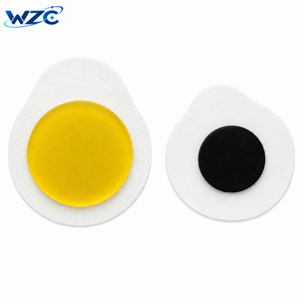
Adhesive-backed bionic friction pad for semiconductor wafer handling
High Friction and Low Adhesion
The pad surface uses a biomimetic microstructure to increase effective friction
between the wafer and the handling surface.
Compared with conventional high-adhesion contact materials, the pad is designed
to provide strong horizontal holding force while keeping the normal pull-off force
relatively low. This combination helps stabilize wafers during movement without
causing excessive sticking during release.
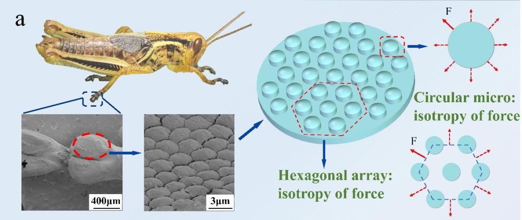
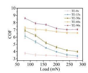
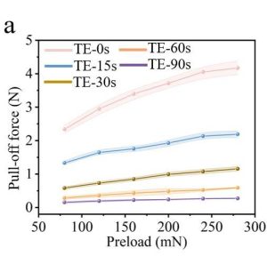
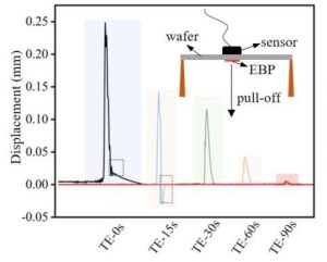
Biomimetic microstructured surface for high friction and controlled adhesion
Standard and Anti-Static Material Options
The adhesive-backed wafer pad is available in both
standard insulating material and
anti-static material.
For applications requiring electrostatic discharge control, the anti-static
version can be selected while maintaining the same microstructured friction
surface and adhesive-backed mounting design.
| Material Option | Typical Volume Resistivity | Application |
|---|---|---|
| Standard | Approx. 2.9 × 10¹⁴ Ω·cm | General wafer handling |
| Anti-Static | 106–109 Ω·cm | ESD-sensitive wafer handling processes |
Standard Adhesive-Backed Pad Sizes
Several standard round pad dimensions are available.
Custom shapes and dimensions can also be supplied according to the
robot finger, end-effector or substrate handling design.
| Diameter | Thickness | Material Options |
|---|---|---|
| 7.0 mm | 1.0 / 1.5 mm | Standard / Anti-Static |
| 8.0 mm | 1.0 / 1.5 mm | Standard / Anti-Static |
| 10.0 mm | 1.0 / 1.5 mm | Standard / Anti-Static |
| Custom | Custom | According to requirement |
Key Features
- High tangential friction for stable wafer handling
- Low normal adhesion for smooth wafer release
- Dry friction design without vacuum contact at the pad surface
- Low surface marking and residue
- Standard and anti-static material options
- Hydrophobic surface with water contact angle greater than 100°
- Suitable for elevated direct-contact temperatures depending on material
- Custom pad diameter, thickness and geometry
- Adhesive-backed structure for simple installation
Typical Applications
The bionic adhesive-backed friction pad can be used in a wide range
of semiconductor and substrate handling systems, including:
- Semiconductor wafer handling robots
- Atmospheric robots
- Vacuum robots
- Wafer aligners
- Robot fingers and end effectors
- Wafer transfer equipment
- Display and glass substrate handling
- Substrate positioning and alignment systems
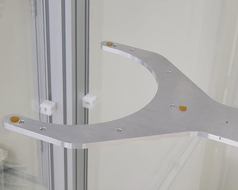
Typical application on wafer handling robot fingers and end effectors
Adhesive-Backed Installation
The adhesive-backed structure is designed for direct attachment to a clean
robot finger or handling surface.
- Clean the mounting surface before installation.
- Carefully remove the adhesive release liner.
- Confirm the correct top and bottom orientation of the pad.
- Install the pad onto the prepared mounting surface.
- Remove particles from the contact surface before use.
Cleanroom handling practices are recommended to prevent contamination of
the microstructured contact surface.
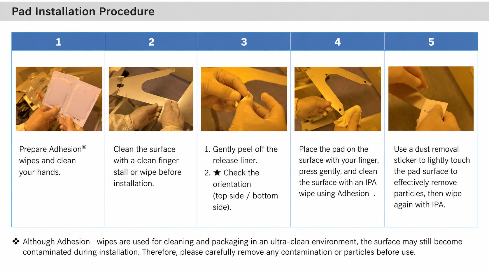
Recommended installation procedure for adhesive-backed friction pads
Custom Bionic Friction Pad Solutions
In addition to standard round pads, customized friction pads can be developed
according to different wafer handling systems and substrate requirements.
- Custom diameter
- Custom thickness
- Round, ring or special geometry
- Standard or anti-static material
- Custom contact height
- Robot finger compatibility
- Custom adhesive-backed design
- Operating temperature requirements
- Wafer or substrate size requirements
For evaluation and quotation, customers can provide the robot finger drawing,
existing pad dimensions, wafer size, operating environment and anti-static
requirements.
Handling and Maintenance
- Handle the pads in a clean environment whenever possible.
- Wear clean gloves during installation and handling.
- Do not touch the microstructured surface with sharp tools.
- Avoid strong rubbing with abrasive materials.
- Keep the pad surface free from particles and contamination.
- Do not reuse a separated adhesive-backed pad without technical evaluation.
- Store unused pads in clean packaging.
Frequently Asked Questions
What is a bionic wafer handling pad?
It is a microstructured friction pad designed to provide high lateral friction
and relatively low normal adhesion for stable wafer and substrate handling.
Is an anti-static version available?
Yes. Standard and anti-static material options are available.
Please specify whether ESD control is required when requesting a quotation.
What standard sizes are available?
Standard round adhesive-backed pads are available in 7 mm, 8 mm and 10 mm
diameters with 1.0 mm and 1.5 mm thickness options.
Can the pad dimensions be customized?
Yes. Diameter, thickness, geometry and material can be customized according
to the robot finger and wafer handling requirements.
Where can the adhesive-backed pad be used?
Typical applications include wafer handling robots, vacuum robots,
atmospheric robots, aligners, robot fingers and custom substrate handling equipment.
Does the pad require vacuum suction?
The friction pad itself relies on surface friction and controlled adhesion
rather than vacuum suction at the contact surface.