12 Inch Sapphire Wafer Specifications
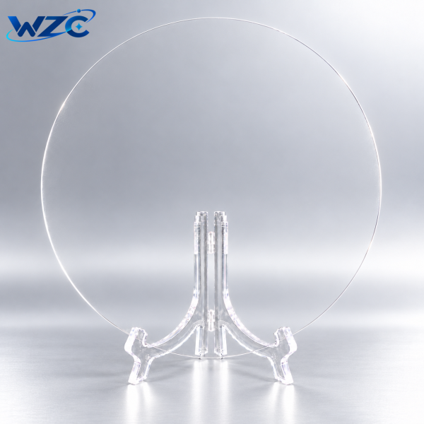
The 12 Inch Sapphire Wafer is a 300 mm single-crystal
Al₂O₃ substrate available with standard and customized crystal orientations,
surface finishes and dimensional specifications.
Material-Semi supplies 300 mm sapphire wafers with C-plane, A-plane,
M-plane and customized orientations. Single-side polished (SSP),
double-side polished (DSP), epi-ready and customized surface configurations
are available according to different semiconductor, optical and research requirements.
Available 12 Inch Sapphire Wafer Options
| Parameter | Available Options |
|---|---|
| Material | Single-Crystal Sapphire (Al₂O₃) |
| Diameter | 300 mm / Custom dimensions available upon request |
| Crystal Orientation | C-Plane (0001) / A-Plane / M-Plane / Custom Orientation |
| Off-Axis | On-axis or customized off-axis angle and direction |
| Thickness | 800 μm / 1000 μm / 1200 μm / Custom |
| Surface Finish | SSP / DSP / Epi-ready / Custom |
| Front Surface | Polished / CMP / Epi-ready |
| Back Surface | Polished / Lapped / Fine Ground / Custom |
| Flat / Notch | Customizable according to crystal orientation and application |
| Edge Profile | T-Type / Custom bevel profile |
| Packaging | Single Wafer Container / Wafer Cassette / FOSB / Custom Packaging |
Typical 12 Inch C-Plane Sapphire Wafer Specification
The following table shows typical 300 mm C-plane sapphire wafer configurations.
Other thicknesses, orientations, surface finishes and off-axis specifications
can be customized according to customer requirements.
| Parameter | Production-1 | Production-2 | Production-3 |
|---|---|---|---|
| Material | >99.999% High-Purity Monocrystalline Al₂O₃ (KY) | ||
| Diameter | 300 ±0.2 mm | ||
| Thickness | 1000 ±50 μm | 800 ±50 μm | 1200 ±50 μm |
| Orientation | C-Plane (0001) | ||
| Off-Set toward M-Axis | 0.0° ±0.3° | ||
| Off-Set toward A-Axis | 0.0° ±0.3° | ||
| Notch Orientation | A-Plane, 0° ±1° | ||
| Notch Depth | 1.0–1.25 mm | ||
| Notch Angle | 85°–95° | ||
| Notch Chamfer | None | ||
| Front Surface | Epi-ready polished, Ra <0.3 nm | ||
| Back Surface | Lapped or fine ground, 0.08 μm < Ra <1.2 μm | ||
| Bevel | T-Type, 200 ±100 μm | ||
| TTV | ≤25 μm | ||
| Bow | ≤35 μm | ≤40 μm | ≤35 μm |
| Warp | ≤120 μm | ≤150 μm | ≤120 μm |
| Chips | ≤0.2 mm | ||
| Laser Mark | None | ||
| Typical Packing | CRC100 packed, 1 pc/box | ||
12 Inch Sapphire Wafer Overview
The 12 Inch Sapphire Wafer is a 300 mm large-diameter
single-crystal Al₂O₃ substrate available for semiconductor, optical,
epitaxial and advanced substrate applications.
Material-Semi supplies both standard and customized 300 mm sapphire wafers.
Crystal orientation, wafer thickness, surface finish, off-axis angle,
notch configuration, edge profile and dimensional tolerances can be
customized according to project requirements.
800 μm, 1000 μm and 1200 μm Thickness Options
Typical 300 mm C-plane sapphire wafers are available with
800 ±50 μm, 1000 ±50 μm
and 1200 ±50 μm thickness specifications.
Other wafer thicknesses and customized dimensions can also be evaluated
according to customer requirements.
C-Plane, A-Plane and M-Plane Sapphire Wafers
Crystal orientation can be selected according to the intended application.
Available options include C-plane, A-plane, M-plane
and other customized crystal orientations.
Both on-axis and customized off-axis sapphire wafers are available.
Customers can specify the required off-axis angle and direction when
requesting a quotation.
SSP, DSP and Epi-Ready Sapphire Wafers
12 inch sapphire wafers can be supplied with
single-side polished (SSP),
double-side polished (DSP) or
epi-ready surface configurations.
The typical specification shown above uses an
epi-ready polished front surface with Ra <0.3 nm
and a lapped or fine-ground backside.
Other combinations, including double-side polishing, can be supplied
according to application requirements.
Custom Sapphire Wafer Options
In addition to standard 300 mm sapphire wafer specifications,
customized sapphire substrates are available for semiconductor,
optical and research applications.
- Custom wafer diameter and dimensions
- Custom wafer thickness
- C-plane, A-plane, M-plane and other crystal orientations
- On-axis and customized off-axis angle and direction
- Single-side polished (SSP)
- Double-side polished (DSP)
- Epi-ready surface finishing
- Custom frontside and backside surface finishing
- Custom flat or notch orientation
- Custom edge profile and bevel
- Custom surface roughness and dimensional tolerances
- Single wafer container, cassette, FOSB and custom packaging
For quotation and technical evaluation, please provide the required
diameter, orientation, thickness, surface finish, off-axis angle,
quantity and any other technical requirements.
Surface Quality and Wafer Geometry
The typical 300 mm sapphire specification provides a total thickness
variation of TTV ≤25 μm.
Typical Bow and Warp requirements vary with wafer thickness.
Frontside surface roughness, backside condition, chips, scratches,
bubbles and pits can be controlled according to the applicable
wafer specification.
How Sapphire Wafers Are Manufactured
Sapphire wafer manufacturing generally includes single-crystal growth,
crystal orientation, slicing, grinding, lapping, polishing,
cleaning and final inspection.
These processing stages are used to control wafer dimensions,
crystal orientation, surface roughness, wafer geometry and edge quality
before final inspection and packaging.
Packaging
The typical 300 mm specification uses
CRC100 packaging with one wafer per box.
Depending on wafer size, quantity and customer requirements,
sapphire wafers can also be supplied in
single wafer containers, wafer cassettes or FOSB packaging.
Customized packaging solutions are available for transportation,
storage and handling requirements.
Frequently Asked Questions
What is a 12 Inch Sapphire Wafer?
It is a large-diameter single-crystal Al₂O₃ substrate with a nominal
diameter of 300 mm.
What thicknesses are available?
Typical thickness options include 800 μm, 1000 μm and 1200 μm.
Other thicknesses can be customized according to customer requirements.
What crystal orientations are available?
C-plane, A-plane, M-plane and customized crystal orientations are available.
On-axis and customized off-axis specifications can also be supplied.
Are SSP and DSP sapphire wafers available?
Yes. Both single-side polished (SSP) and double-side polished (DSP)
sapphire wafers are available, together with epi-ready surface finishing.
What is the typical front surface roughness?
The typical epi-ready specification has a front surface roughness of
Ra <0.3 nm.
Can the wafer thickness and orientation be customized?
Yes. Wafer thickness, crystal orientation, off-axis angle,
surface finish, notch configuration, edge profile and other dimensions
can be customized according to project requirements.
Is FOSB packaging available for sapphire wafers?
Yes. FOSB packaging can be supplied according to wafer size,
quantity and customer packaging requirements.
Single wafer containers and wafer cassettes are also available.