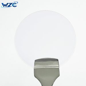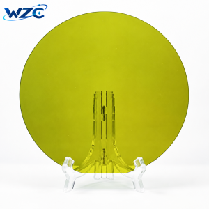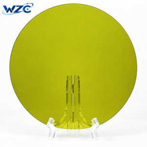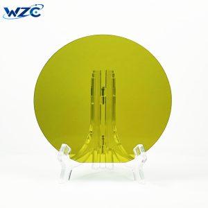
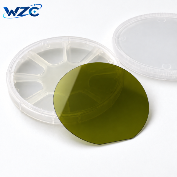
2 Inch 4H-N SiC Wafer Specifications
The 2 Inch 4H-N SiC Wafer is a 50.8 mm N-type 4H silicon carbide substrate
available in Production Grade, Research Grade and Dummy Grade.
Standard wafers feature a diameter of 50.8 ± 0.38 mm and a thickness of
330 ± 25 μm. Both on-axis and 4° off-axis orientation options are available.
| Parameter | Specification |
|---|---|
| Material | 4H Silicon Carbide (4H-SiC) |
| Conductivity Type | N-Type |
| Diameter | 50.8 ± 0.38 mm |
| Thickness | 330 ± 25 μm |
| Grade | Production Grade / Research Grade / Dummy Grade |
| Wafer Orientation | On-axis <0001> ±0.5° or 4.0° off-axis toward <11-20> ±0.5° |
| Resistivity | 0.015–0.028 Ω·cm |
| Micropipe Density | Production Grade: ≤5 cm-2 Research Grade: ≤15 cm-2 Dummy Grade: ≤50 cm-2 |
| Primary Flat Orientation | {10-10} ±5.0° |
| Primary Flat Length | 15.9 ± 1.7 mm |
| Secondary Flat Length | 8.0 ± 1.7 mm |
| Secondary Flat Orientation | Silicon face up: 90° CW from primary flat ±5.0° |
| Edge Exclusion | 1 mm |
| TTV | ≤15 μm |
| Bow | ≤25 μm |
| Warp | ≤25 μm |
| Surface Finish | Polish / CMP |
| Polished Surface Roughness | Ra ≤1 nm |
| CMP Surface Roughness | Ra ≤0.5 nm |
2 Inch 4H-N Silicon Carbide Wafer Overview
The 2 inch 4H-N SiC wafer is a 50.8 mm N-type 4H silicon carbide substrate
available with controlled electrical, dimensional and surface specifications.
The standard wafer thickness is 330 ± 25 μm, with resistivity specified at
0.015–0.028 Ω·cm.
Production Grade, Research Grade and Dummy Grade options are available.
Different grades provide different limits for micropipe density and visual defects,
allowing the wafer specification to be selected according to different technical requirements.
On-Axis and 4° Off-Axis 4H-N SiC Wafers
The 2 inch 4H-N SiC substrate can be supplied with an
on-axis <0001> ±0.5° orientation or with a
4.0° off-axis toward <11-20> ±0.5° orientation.
Customers should specify the required crystal orientation when requesting a quotation
or confirming the wafer specification.
Production, Research and Dummy Grades
Three wafer grades are available for the 2 inch 4H-N SiC substrate:
Production Grade, Research Grade and
Dummy Grade.
The specified micropipe density limits are ≤5 cm-2 for Production Grade,
≤15 cm-2 for Research Grade and ≤50 cm-2 for Dummy Grade.
The grades also have different visual defect acceptance criteria.
Visual Defect Criteria
| Inspection Item | Production Grade | Research Grade | Dummy Grade |
|---|---|---|---|
| Cracks | None | None | 1 allowed, ≤1 mm |
| Hex Plates | Cumulative area ≤1% | Cumulative area ≤1% | Cumulative area ≤3% |
| Polytype Areas | None | Cumulative area ≤2% | Cumulative area ≤5% |
| Scratches | 3 scratches, cumulative length ≤1× wafer diameter | 5 scratches, cumulative length ≤1× wafer diameter | 8 scratches, cumulative length ≤1× wafer diameter |
| Edge Chips | None | 3 allowed, ≤0.5 mm each | 5 allowed, ≤1 mm each |
| Contamination | None | None | None |
Note: Defect limits apply to the entire wafer surface except for the edge exclusion area.
Surface Finish and Roughness
Polished and CMP surface finishes are available for the 2 inch 4H-N SiC wafer.
The specified polished surface roughness is Ra ≤1 nm,
while the CMP surface roughness is Ra ≤0.5 nm.
Wafer Geometry
Wafer geometry is controlled with a total thickness variation
TTV ≤15 μm, Bow ≤25 μm and
Warp ≤25 μm. The specified edge exclusion is 1 mm.
How SiC Wafers Are Manufactured
SiC wafer manufacturing generally includes crystal growth, crystal orientation,
wafer slicing, grinding, polishing, chemical mechanical polishing (CMP),
cleaning and final inspection.
These processing stages are used to control wafer dimensions, surface roughness,
flatness and defect quality before the substrate is prepared for delivery.
The final acceptance requirements depend on the selected wafer grade and specification.
Custom 2 Inch 4H-N SiC Wafer Requirements
When requesting a quotation, please specify the required wafer grade,
on-axis or off-axis orientation, surface finish, quantity and any additional
technical requirements.
Frequently Asked Questions
What is the diameter of a 2 inch 4H-N SiC wafer?
The specified wafer diameter is 50.8 ± 0.38 mm.
What is the standard thickness?
The standard thickness is 330 ± 25 μm.
What is the resistivity of the 4H-N SiC substrate?
The specified resistivity is 0.015–0.028 Ω·cm.
Is 4° off-axis available?
Yes. The specification includes a 4.0° off-axis orientation toward
<11-20> with a tolerance of ±0.5°.
Is an on-axis 4H-N SiC wafer available?
Yes. An on-axis <0001> ±0.5° specification is also listed.
What surface finishes are available?
Polished and CMP surface finishes are available. The specified roughness is
Ra ≤1 nm for polished surfaces and Ra ≤0.5 nm for CMP surfaces.
What wafer grades are available?
Production Grade, Research Grade and Dummy Grade are available,
with different micropipe density and visual defect acceptance limits.
Explore more
SiC Wafers
from Material-Semi.