


Introduction
In semiconductor manufacturing, wafer thickness uniformity is a critical parameter that affects lithography, bonding, polishing, and overall device yield. One of the most commonly used parameters to evaluate wafer thickness uniformity is TTV (Total Thickness Variation).
This article explains what TTV means, how it is measured, and why it matters for semiconductor wafer applications.
What Is TTV?

What Does TTV Mean?
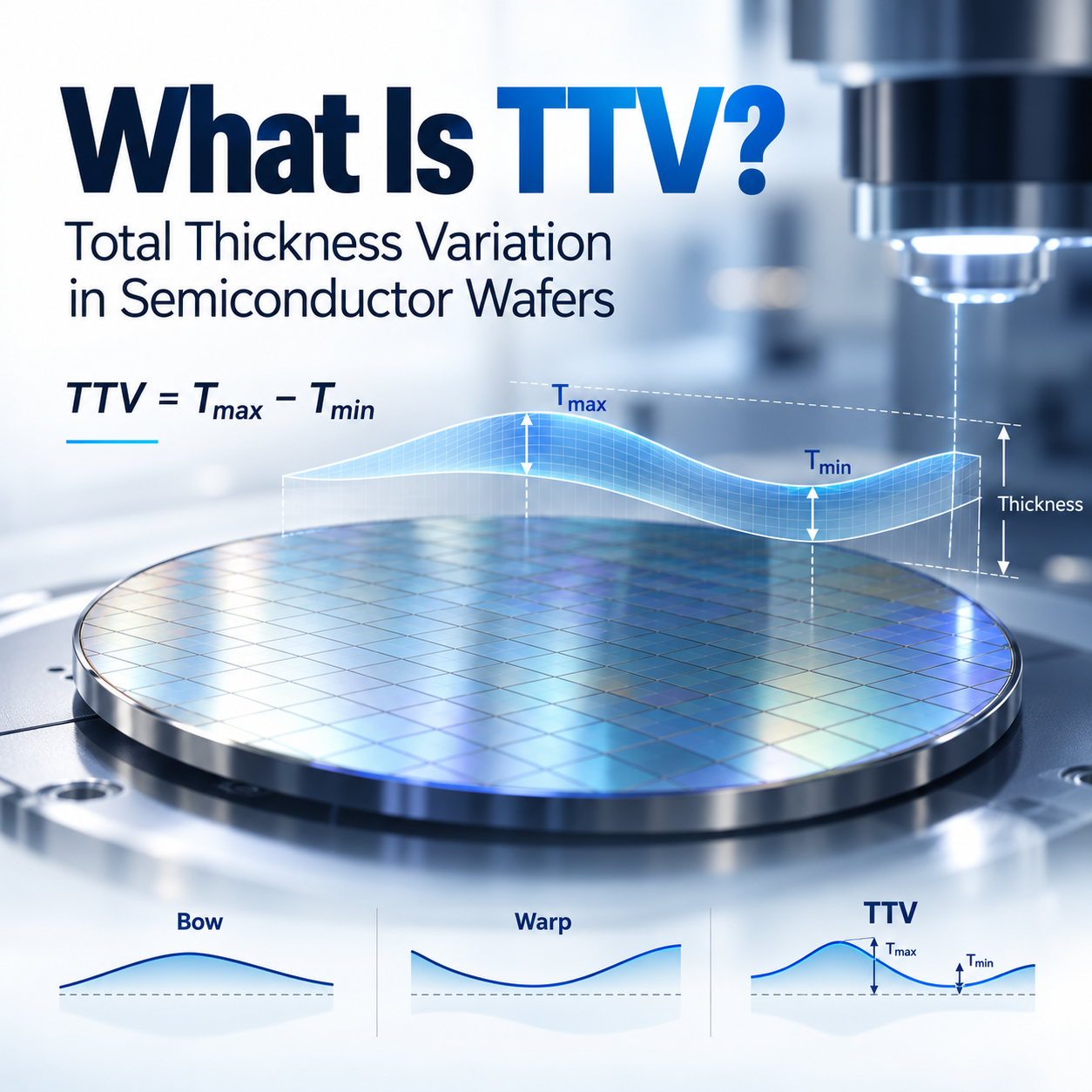
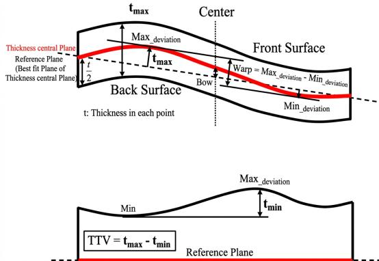
TTV (Total Thickness Variation) describes the difference between the maximum and minimum thickness values measured across a wafer surface.
Mathematically:
TTV = Tmax − Tmin
where:
- Tmax = maximum measured wafer thickness
- Tmin = minimum measured wafer thickness
The measurement is normally performed within a defined measurement area, excluding edge regions and other restricted zones.
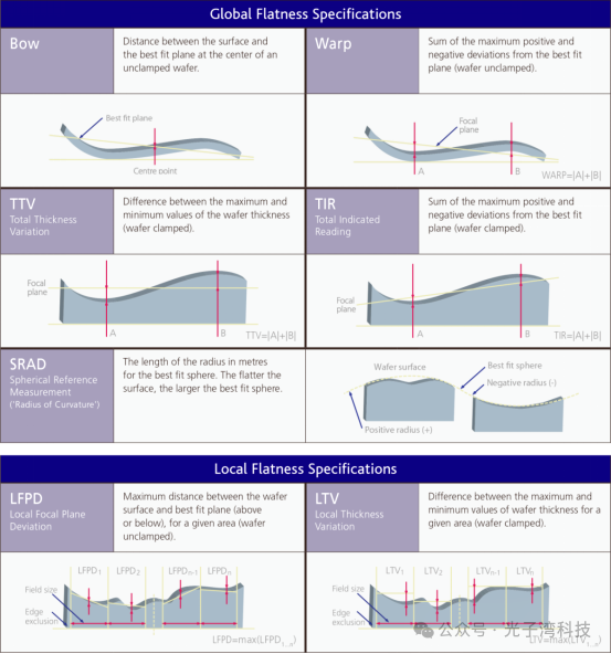
TTV represents the thickness uniformity of the wafer body and should not be confused with wafer shape parameters such as Bow or Warp.
TTV vs Bow vs Warp
Difference Between TTV, Bow and Warp
Although TTV, Bow, and Warp are all wafer geometry parameters, they describe different characteristics.
| Parameter | Description |
|---|---|
| TTV | Variation of wafer thickness across different locations |
| Bow | Overall curvature of a wafer relative to its reference plane |
| Warp | Total deviation of a wafer surface from the ideal reference plane |
How Is TTV Measured?
Common Wafer TTV Measurement Methods
Optical Interferometry
Uses light interference patterns to determine wafer thickness variations with high precision.
Advantages:
- Non-contact measurement
- High accuracy
- Suitable for advanced semiconductor wafers
Capacitive Measurement
Uses changes in electrical capacitance to calculate wafer thickness.
Advantages:
- Fast measurement speed
- Suitable for automated inspection systems
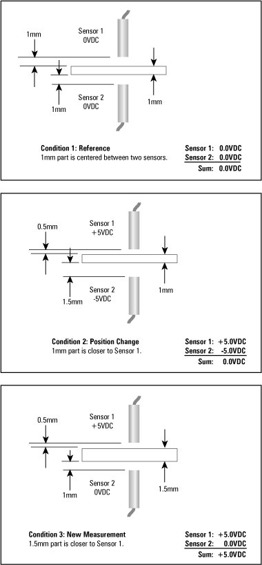
Confocal and Laser-Based Measurement
Measures the distance between the upper and lower wafer surfaces using optical sensors.
Why Does TTV Matter in Semiconductor Manufacturing?
Impact of High TTV
1. Lithography and Focus Control
High TTV can introduce surface height variation, affecting focus accuracy during lithography processes.
2. CMP Process Stability
Thickness variation increases polishing challenges and may lead to uneven material removal.
3. Wafer Bonding
For wafer bonding applications, excessive TTV can cause local gaps and bonding defects.
4. Device Yield
Poor wafer thickness uniformity may contribute to process variation and reduced yield.
Typical TTV Requirements
The acceptable TTV specification depends on:
- Wafer diameter
- Material type
- Crystal orientation
- Application requirements
- Manufacturing process
For advanced semiconductor applications, tighter TTV control is generally required, while research-grade wafers may allow wider specifications.
| Wafer Type | Typical Consideration |
|---|---|
| Silicon wafer | Very tight thickness uniformity requirements |
| SiC wafer | Depends on substrate grade and device requirements |
| Sapphire wafer | Related to polishing quality and application |
| SOI/LNOI | Thickness control is critical for device performance |
Factors Affecting Wafer TTV
TTV can be influenced by:
- Crystal growth quality
- Wafer slicing process
- Grinding and lapping conditions
- Double-side polishing process
- Surface finishing technology
Manufacturers improve TTV through optimized polishing processes, precise equipment control, and advanced measurement systems.
Conclusion
TTV is an important wafer specification used to evaluate thickness uniformity and manufacturing consistency.
Understanding TTV, together with parameters such as Bow, Warp, surface roughness, and flatness, helps engineers select suitable semiconductor substrates for different applications.
Material-Semi provides semiconductor substrates including silicon carbide wafers, sapphire wafers, and other advanced materials with customized specifications.
Contact our team to discuss your wafer requirements.