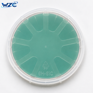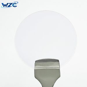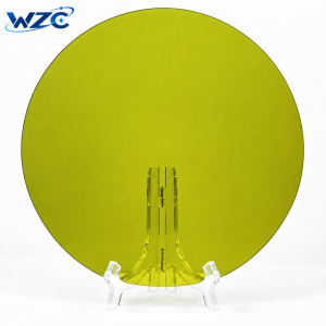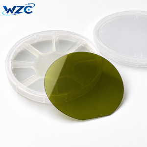
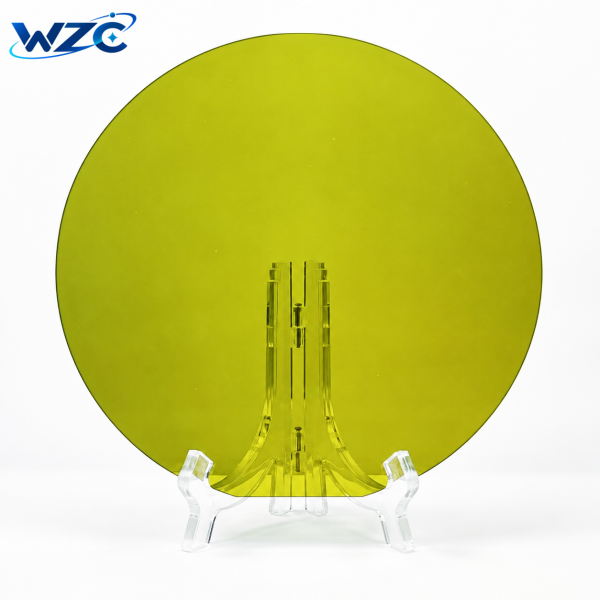
8 Inch 4H-N SiC Wafer Specifications
The 8 Inch 4H-N SiC Wafer is a 200 mm N-type 4H silicon carbide substrate
available in Zero MPD Production Grade (Z Grade) and Dummy Grade (D Grade).
The substrate features a 4.0° off-axis orientation toward <11-20> ±0.5°
with polished and CMP surface options.
| Parameter | Z Grade | D Grade |
|---|---|---|
| Material | 4H Silicon Carbide (4H-SiC) | |
| Conductivity Type | N-Type / Conductive | |
| Diameter | 199.5–200.0 mm | 199.5–200.0 mm |
| Thickness | 500 ±25 μm | 500 ±25 μm |
| Wafer Orientation | 4.0° off-axis toward <11-20> ±0.5° | |
| Micropipe Density | ≤0.2 cm-2 | ≤5 cm-2 |
| Resistivity | 0.015–0.025 Ω·cm | 0.015–0.028 Ω·cm |
| Notch Orientation | {10-10} ±5.0° | |
| Edge Exclusion | 3 mm | |
| LTV | ≤5 μm | ≤10 μm |
| TTV | ≤10 μm | ≤15 μm |
| Bow | ±35 μm | ±50 μm |
| Warp | 70 μm | 100 μm |
| Polished Surface Roughness | Ra ≤1 nm | |
| CMP Surface Roughness | Ra ≤0.2 nm | Ra ≤0.5 nm |
| TSD | ≤300 cm-2 | — |
| Packaging | Multi-wafer cassette / Single wafer container | |
8 Inch 4H-N Silicon Carbide Wafer Overview
The 8 Inch 4H-N SiC Wafer is a conductive 200 mm 4H silicon carbide substrate
designed for large-diameter semiconductor processing and material development.
Zero MPD Production Grade and Dummy Grade options are available with different
requirements for micropipe density, wafer geometry and visual defects.
The substrate features a 4.0° off-axis orientation toward <11-20> ±0.5°.
Z Grade resistivity is specified at 0.015–0.025 Ω·cm,
while D Grade is specified at 0.015–0.028 Ω·cm.
Zero MPD Production Grade and Dummy Grade
Zero MPD Production Grade (Z Grade) provides tighter control over
micropipe density, wafer geometry and surface quality. The specified micropipe density
is ≤0.2 cm-2.
Dummy Grade (D Grade) is available with wider acceptance limits,
with micropipe density specified at ≤5 cm-2.
4° Off-Axis 200 mm 4H-N SiC Substrate
The 8 inch 4H-N SiC wafer is specified with a
4.0° off-axis angle toward <11-20> ±0.5°.
The notch orientation is specified as {10-10} ±5.0°.
Wafer Geometry Control
For Z Grade substrates, wafer geometry is specified at
LTV ≤5 μm, TTV ≤10 μm,
Bow ±35 μm and Warp 70 μm.
For D Grade substrates, the corresponding values are
LTV ≤10 μm, TTV ≤15 μm,
Bow ±50 μm and Warp 100 μm.
Surface Finish and Roughness
Polished and CMP surface finishes are available.
The polished surface roughness is specified at Ra ≤1 nm.
CMP surface roughness is specified at Ra ≤0.2 nm for Z Grade
and Ra ≤0.5 nm for D Grade.
Visual Defect Criteria
| Inspection Item | Z Grade | D Grade |
|---|---|---|
| Edge Cracks | None | Cumulative length ≤30 mm; single length ≤2 mm |
| Hex Plates | Cumulative area ≤0.05% | Cumulative area ≤0.1% |
| Polytype Areas | None | Cumulative area ≤3% |
| Visual Carbon Inclusions | Cumulative area ≤0.05% | Cumulative area ≤3% |
| Si Surface Scratches | None | Cumulative length ≤1× wafer diameter |
| Edge Chips | No chips with width ≥0.2 mm and depth ≥0.2 mm | ≤9 allowed, each ≤1 mm |
| Surface Contamination | None | None |
How SiC Wafers Are Manufactured
SiC wafer manufacturing generally includes crystal growth, crystal orientation,
slicing, grinding, polishing, chemical mechanical polishing (CMP),
cleaning and final inspection.
These processing steps are used to control wafer dimensions, surface roughness,
wafer geometry and defect quality before final inspection and packaging.
Packaging
8 inch 4H-N SiC wafers can be supplied in a
multi-wafer cassette or single wafer container
according to order quantity and packaging requirements.
Custom 8 Inch 4H-N SiC Wafer Requirements
When requesting a quotation, please specify the required wafer grade,
surface finish, quantity and any additional dimensional or defect requirements.
Frequently Asked Questions
What is an 8 Inch 4H-N SiC Wafer?
It is a conductive 4H silicon carbide substrate with a nominal diameter of 200 mm
and N-type electrical characteristics.
What is the diameter of the 8 inch SiC substrate?
The specified diameter range is 199.5–200.0 mm.
What thickness is available?
Both Z Grade and D Grade are specified at 500 ±25 μm.
What is the resistivity?
Z Grade is specified at 0.015–0.025 Ω·cm,
while D Grade is specified at 0.015–0.028 Ω·cm.
Is the wafer 4° off-axis?
Yes. The specified orientation is
4.0° off-axis toward <11-20> ±0.5°.
What CMP surface roughness is available?
CMP surface roughness is specified at Ra ≤0.2 nm for Z Grade
and Ra ≤0.5 nm for D Grade.
What grades are available?
Zero MPD Production Grade (Z Grade) and Dummy Grade (D Grade) are available
according to this product specification.